Nexa3D Completes Acquisition of Essentium 🎉 Read the full story!

Electrostatically dissipative (xESD) 3D printing resin

Challenge

Long lead times and the costs associated with machined, bespoke semiconductor component carriers prompted the Customer to explore Additive Manufacturing (AM) technologies. The goal was to accelerate new product introduction cycles and avoid instances of having to replace the entire testing equipment due to the redesign of a single component carrier.

The Customer had specific requirements for the AM equipment and material options, including:

  1. The ability to achieve an exceptionally high level of feature resolution
  2. Static dissipative material capability

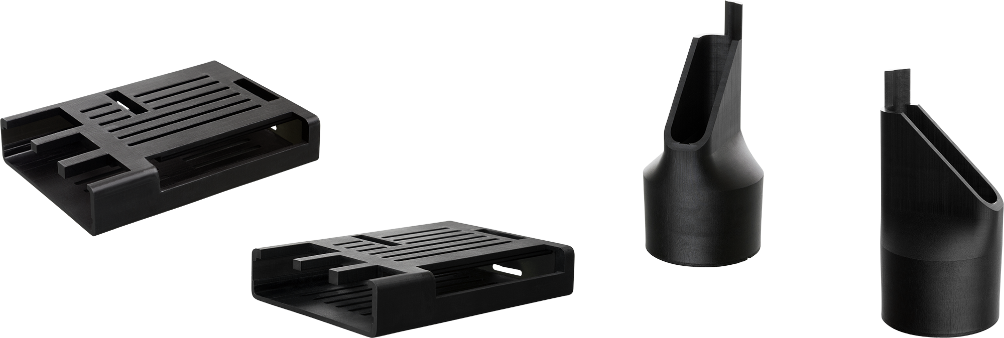
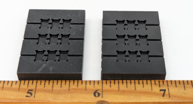
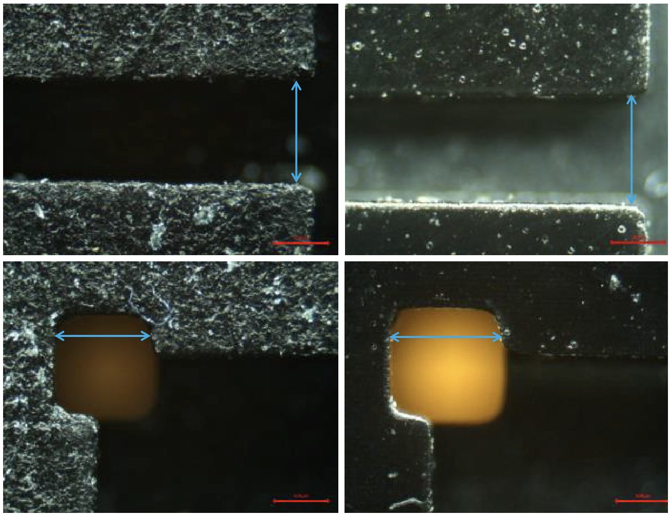
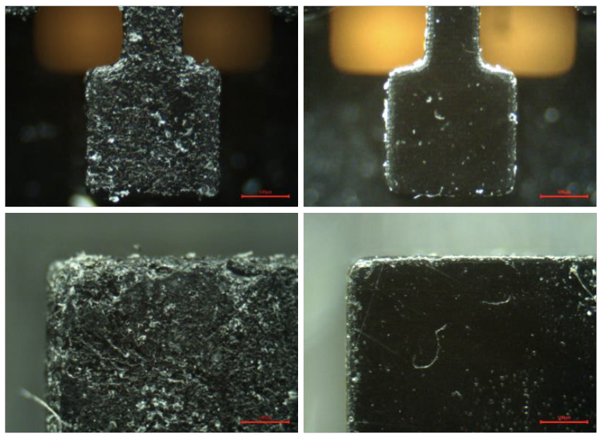
The Customer faced a challenge in finding the right combination of electrostatic discharge (ESD) materials and AM equipment. The options they previously explored relied on filament-based AM, but these options were unable to meet the intricate feature requirements. The capabilities of Fused Filament Fabrication (FFF) equipment, as shown in Figure 1, were not sufficient to achieve the necessary level of precision. As a result, the components produced by FFF machines were unusable. Consequently, the Customer actively sought out an alternative AM process capable of accommodating both high resolution and ESD requirements.

CAD model of the part
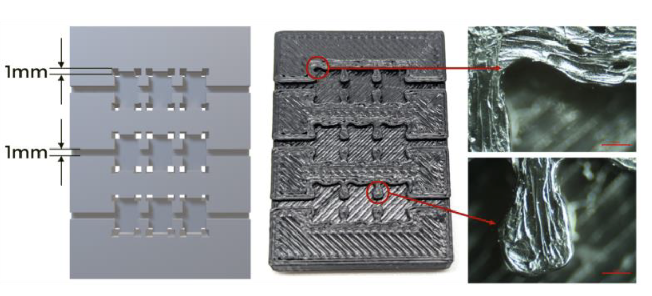
Figure 1: CAD model of the part and the slightly modified version built using FFF. Photo of the FFF part shows inadequate resolution of the features, which renders parts unusable.

Customer

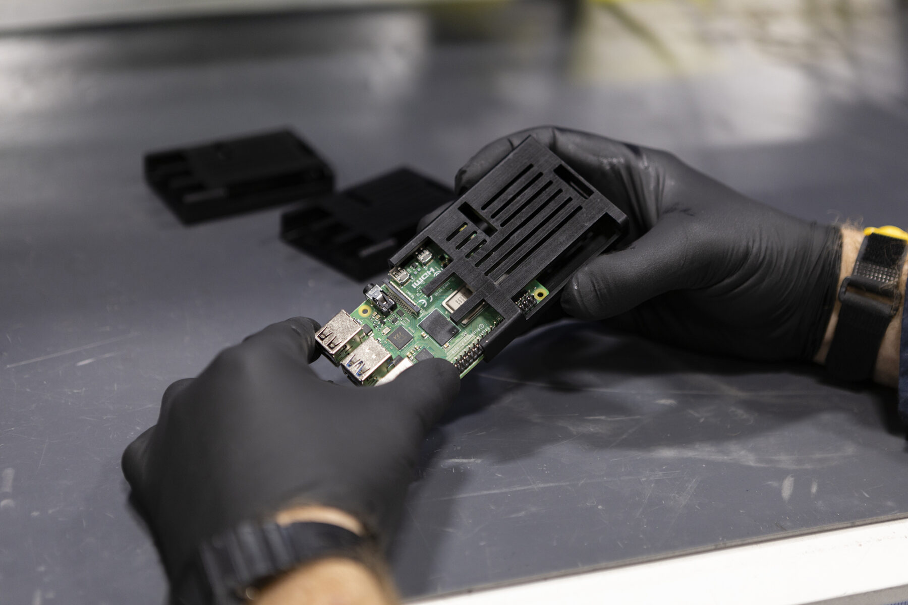
Confidential customer (“Customer”) is a manufacturer of ultra-miniature semiconductor components for medical, aerospace and defense, and industrial markets.

Industry

Semiconductor

Technology

Vat Photopolymerization

Material

xESD

Challenge

  • Long lead times & cost for bespoke semiconductor component carriers
  • Inability of FFF to achieve necessary precision levels
  • Solution

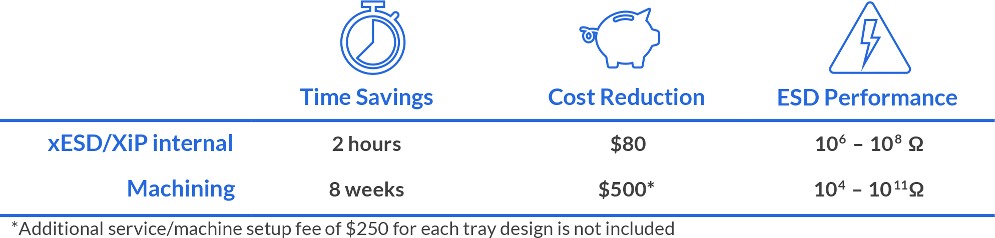
    • Use xESD and XiP for part
      fabrication

Results

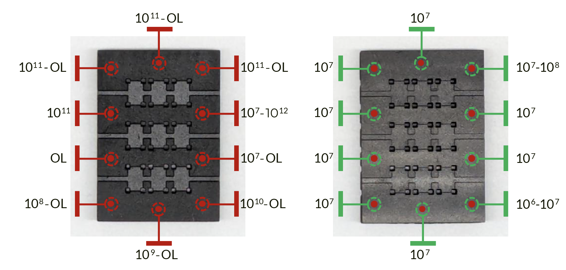
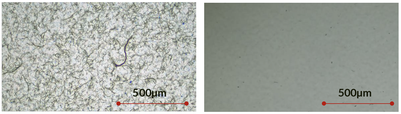
  • Nano-Uniform ESD performance
  • Exceptional feature resolution
  • Outstanding surface finish

Impact

  • Reduction in lead time from
    8 weeks to 2 hours
  • 84% cost reduction
  • Higher-accuracy parts with finer
    detail and resolution

xESD material

Solution

To address the demand for the high resolution static dissipative components, the Customer turned to static-dissipative resins for vat photopolymerization systems, which offer superior resolution compared to FFF. The Customer conducted a comparative evaluation of Nexa3D’s xESD formulated by Mechnano for ultrafast LSPc 3D printing technology and a resin and SLA machine combination offered by a competitor in the market (“Competitor”).

Results

Figure 2 shows the fabricated semiconductor component carriers evaluated between a Competitor and xESD, as indicated. The parts surpassed the resolution capabilities of the FFF hardware, as anticipated. The 1 mm pockets and channels were clearly defined and appeared to be functional upon visual examination. It is worth noting that the surface finish was noticeably different – the Competitor part had rougher surface quality, while the part fabricated on Nexa3D’s XiP desktop printer with xESD had a smooth, nearly glassy surface finish.

hotos of semiconductor components carrier fabricated using Competitor and xESD/XiP
Figure 2: Photos of semiconductor components carrier fabricated using Competitor and xESD/XiP.

In order to ensure that the feature sizes and static dissipative performance meet the requirements of the Customer’s application, the next step involved conducting microscopy analysis and surface resistivity measurements. Figure 3 shows microscopy images of the fabricated components. When comparing the Competitor parts to the desired specifications, it was observed that there was a roughly 7% reduction in channel width and a 10% decrease in pocket size. The part fabricated using xESD exhibited a less than 1% increase in channel width and about a 3% increase in pocket size. The reduced pocket sizes in the Competitor parts rendered them unusable. In contrast, the slight increase in size observed in the part fabricated using xESD did not compromise the performance of the component. Fabricating high resolution parts is essential for the Customer due to the ongoing downsizing of semiconductor components, resulting in an increasing need for improved precision in their manufacturing processes.

Microscopy images of channels (top) and pockets (bottom) display significant deviation from CAD model
Figure 3: Microscopy images of channels (top) and pockets (bottom) display significant deviation from CAD model in Competitor parts compared to xESD.

The static dissipative properties were evaluated according to the ANSI ESD S11.13 – Standard Test Method for the Protection of Electrostatic Discharge Susceptible Items – Two-Point Resistance Measurement. Measurements were taken at 10 locations on the part’s surface. Three separate specimens were tested for each resin and the values were reported in ranges. The measurement map for both the Competitor and xESD is shown in Figure 4. The Competitor part had resistance ranging from 107 to 1011 Ω, with multiple instances where an “Open Loop” reading was observed. An “Open Loop” or OL reading indicates that the tested component lacks continuity and possesses infinite resistance. Infinite resistance implies the absence of an electric current flowing through the component. In contrast, parts fabricated with xESD displayed highly precise surface resistance measurements, ranging from 106 to 108 Ω. The resistivity at any specific location on the component either varied by one order of magnitude or remained constant at 107 Ω.

SD measurements map showing the range of resistance values collected from each location
Figure 4: ESD measurements map showing the range of resistance values collected from each location. The Competitor part failed to deliver acceptable levels of ESD protection. The xESD part displayed nano-uniform ESD performance throughout the component.

The observed variations in the static dissipative performance can be attributed to the noticeable disparities in the surface quality of the components and quality of the CNTs dispersion in a resin.

As noted, the Competitor components exhibited visibly rougher surface finish in contrast to the smooth surfaces of xESD parts. Microscopy images (see Figure 5) further illustrate this discrepancy. The Competitor part displayed an exceedingly rough surface finish with noticeable pitting occurring in multiple locations. When the electrodes of the resistance probe came into contact with the surface of this component, the presence of roughness restricted the effective connection between materials to only a portion of the available area. As a result, current flowed solely through the true contact areas, while the roughness introduced contact resistance. This contact resistance explained the significant differences observed in the surface resistance measurements obtained from the Competitor part when compared to uniform measurements of xESD components.

Microscopy images of the part surface for the Competitor and xESD
Figure 5: Microscopy images of the part surface for the Competitor and xESD, as indicated. The Competitor part has extremely rough surface finish compared to xESD. Surface roughness plays a crucial role in discrepancies of the static dissipative readings collected from Competitor parts.

Dispersion quality served as another factor contributing to the discrepancy in ESD readings. To illustrate this point, optical microscopy images of Competitor and xESD resins are presented in Figure 6. The images clearly indicate that Competitor resin contained a higher concentration of CNTs compared to xESD. The crucial distinction between the two was the inferior dispersion quality observed in the Competitor resin, where a significant number of CNT bundles coexisted alongside regions lacking CNTs.

In contrast, microscopy of xESD demonstrates a well-distributed and uniform dispersion of CNTs without the formation of CNT bundles or areas devoid of CNTs due to integration of xESD’s proprietary discrete, dispersed, and functionalized CNTs (D’Func) into the resin.

ptical microscopy images of the Competitor and xESD resins
Figure 6: Optical microscopy images of the Competitor and xESD resins, as indicated. The dispersion quality of the Competitor resin is inferior to the quality of xESD, which contributes to discrepancy in the ESD readings.

Achieving high-quality dispersion is imperative to ensure homogeneous distribution of conductive additives within the polymer matrix. This distribution enables formation of conductive bridges, consisting of overlapping electronic structures, which facilitate electron transfer. The presence of regions without CNTs and highly concentrated areas adversely affects the uniform distribution of the conductive filler in the manufactured component, resulting in sections with inconsistent conductivity.

Impact

Using xESD and XiP yields numerous benefits including a smooth surface finish, consistent surface resistance, and exceptional feature resolution. Deploying xESD and XiP in house allows the Customer to reduce the cost associated with design iterations and enables the optimization of tooling. The transition from outsourced machining services to in-house fabrication using xESD and XiP, allows the Customer to achieve an impressive reduction in part lead time from 8 weeks to a mere 2 hours and a substantial cost reduction of 84%. Ultimately, this powerful combination enables the Customer to rapidly produce functional semiconductor component carriers, while minimizing both time and expenses as opposed to conventional manufacturing approaches.

xESD Performance Chart